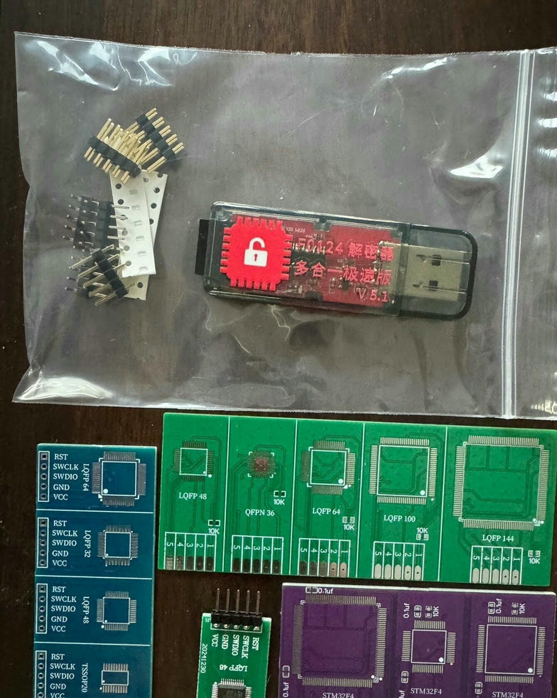
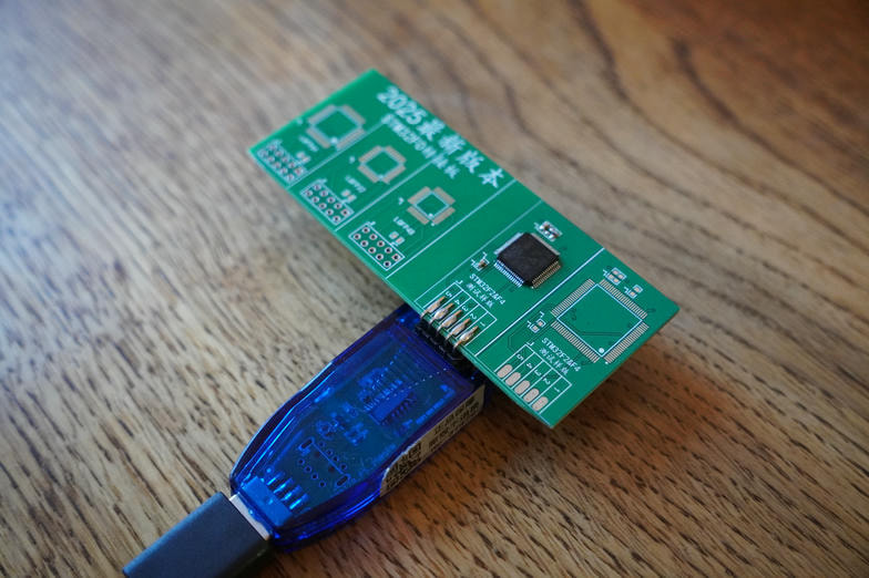
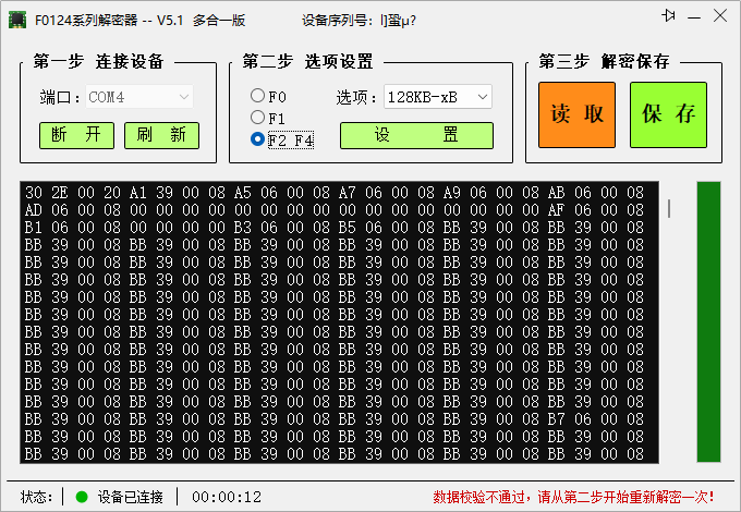
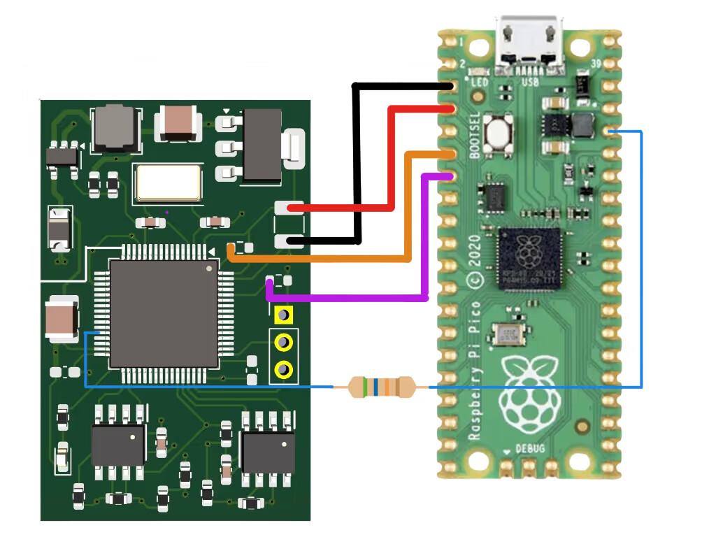
It has been a while I wanted to summarize some attacks on the STM32 somewhere, and looking at a presentation at Hardwear.io 2025 in USA, I was hopping to have time doing it, then got busy but → better writing it now than never!
STM32 microcontrollers from STMicroelectronics are everywhere: industrial controllers, medical devices, IoT gateways, automotive ECUs, consumer electronics. Their popularity also makes them a prime target for security researchers and attackers alike. At the heart of STM32 firmware confidentiality lies the Readout Protection (RDP) mechanism, a hardware feature designed to prevent unauthorized access to the internal flash memory via debug interfaces (SWD/JTAG).
But over the past years, the research community has systematically tackled this protection, layer by layer. This post traces that journey from the first UV-C optical attacks to the latest CPU state tracing technique presented at Hardwear.io USA 2025, so we get some references in here.
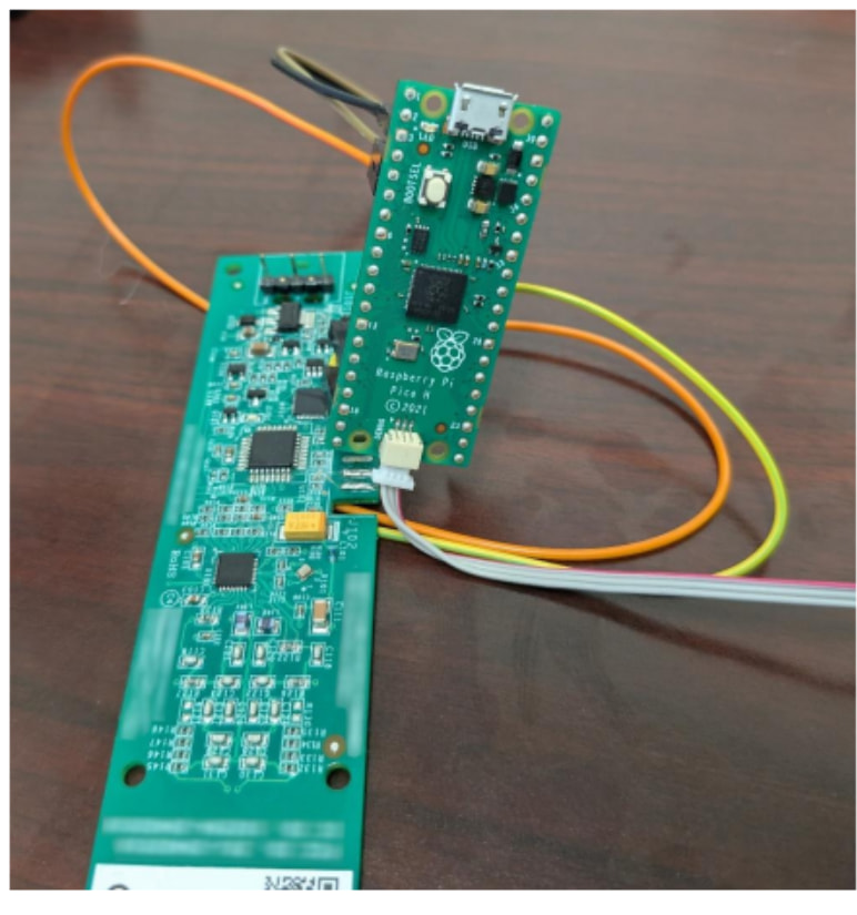
(source: https://hardwear.io/usa-2025/presentation/TraceRip-Hardwear.pdf)
So let’s talk about RDP first, and what it means to us to refresh our mind.
The RDP Model: the 3 Levels
On STM32 platforms, we can find mainly 3 readout level:
- RDP Level 0: no protection. flash fully accessible via debug interface,
- RDP Level 1: debug connection allowed, but flash reads via debugger trigger a HardFault and lock the flash interface. SRAM and peripherals remain accessible. Most commonly deployed level,
- RDP Level 2: full lockdown. Debug interface permanently disabled. ST warns this is irreversible (with caveats, as we’ll see)
The critical assumption underpinning RDP Level 1: if you can’t read flash through the debugger, the firmware is safe. As research has shown, that assumption is fundamentally flawed.
Evolution of attacks
2017: Shedding too much Light on a Microcontroller’s Firmware Protection(Obermaier & Tatschner)
The foundational work came from Johannes Obermaier, and Stefan Tatschner at Fraunhofer AISEC, published at USENIX WOOT 2017. Their paper “Shedding too much Light on a Microcontroller’s Firmware Protection” targeted the STM32F0 and revealed three weaknesses:
1. UV-C Optical Fault Injection (Level 2 → Level 1 downgrade) RDP level is stored in option bytes in flash. Exposing a decapped chip to UV-C light selectively discharges protection bits, downgrading Level 2 to Level 1. Invasive (requires decapsulation), but the first demonstrated path from “permanently locked” to “attackable.”
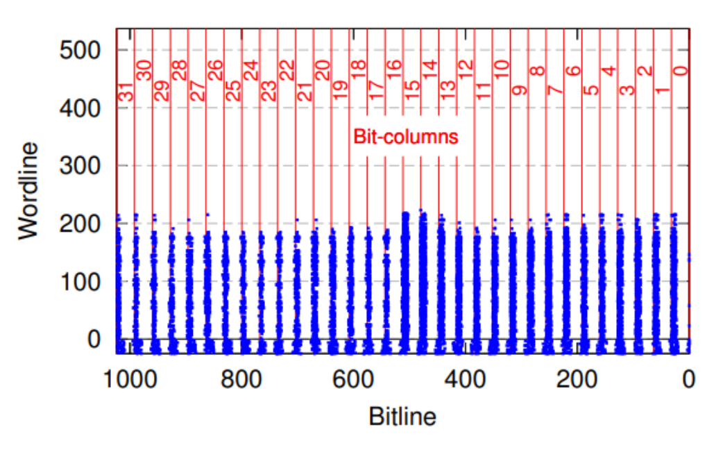
(source: https://www.usenix.org/system/files/conference/woot17/woot17-paper-obermaier.pdf)
2. Debug Interface Race Condition (Level 1 bypass on STM32F0) On the STM32F0, the very first bus access after debugger connection succeeds before protection kicks in. Firmware extractable one word at a time: power cycle, connect, read one word, repeat.
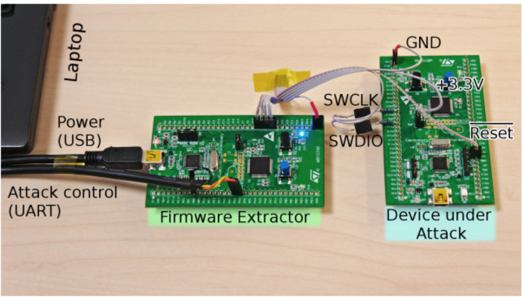
(source: https://www.usenix.org/system/files/conference/woot17/woot17-paper-obermaier.pdf)
3. Cold-Boot Stepping (Level 1 data leakage via SRAM) If firmware performs a CRC integrity check at boot, intermediate CRC values pass through SRAM. Since SRAM remains readable under RDP Level 1, an attacker can power-cycle with precise timing, read the CRC state, and back-calculate flash contents byte by byte.
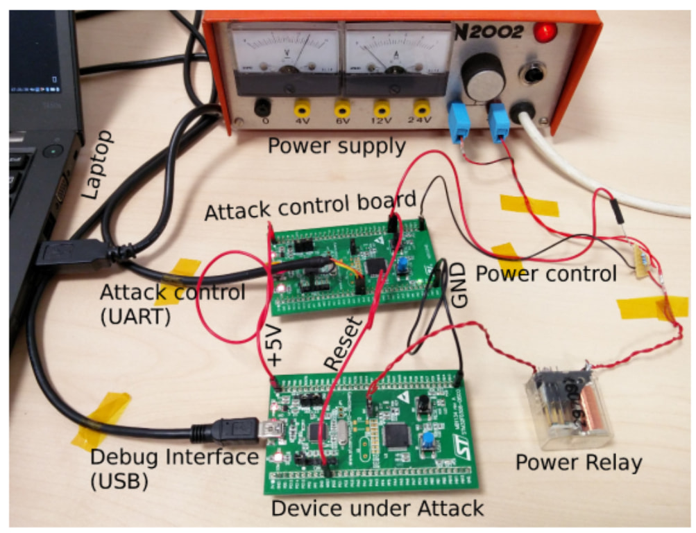
(source: https://www.usenix.org/system/files/conference/woot17/woot17-paper-obermaier.pdf)
This last technique doesn’t require any silicon bugs → it exploits a design-level assumption: that leaking processor state and SRAM is not equivalent to leaking flash.
The paper can be read there: https://www.usenix.org/system/files/conference/woot17/woot17-paper-obermaier.pdf
2020: Exception(al) Failure - Breaking the STM32F1 Read-Out Protection (Obermaier, Schink)
Targeting the STM32F1 series, vulnerability CVE-2020-8004 exploited how the Cortex-M3 fetches exception vectors. While data reads via the DCode bus are blocked by RDP Level 1, the ICode bus used for instruction and vector fetches is not blocked. By manipulating the vector table and triggering exceptions, roughly 90% of flash could be extracted without glitching.
In parallel, the Flash Patch/Breakpoint (FPB) unit was abused with a voltage glitch to redirect the reset vector for full flash extraction on STM32F1.
Blog post: Exception(al) Failure - Breaking the STM32F1 Read-Out Protection | blog.zapb.de
WOOT’20 Slides: https://www.usenix.org/system/files/woot20-paper-obermaier.pdf
2021–2024: The glitching era
As earlier logic-level exploits got patched, researchers turned to voltage fault injection (VFI).
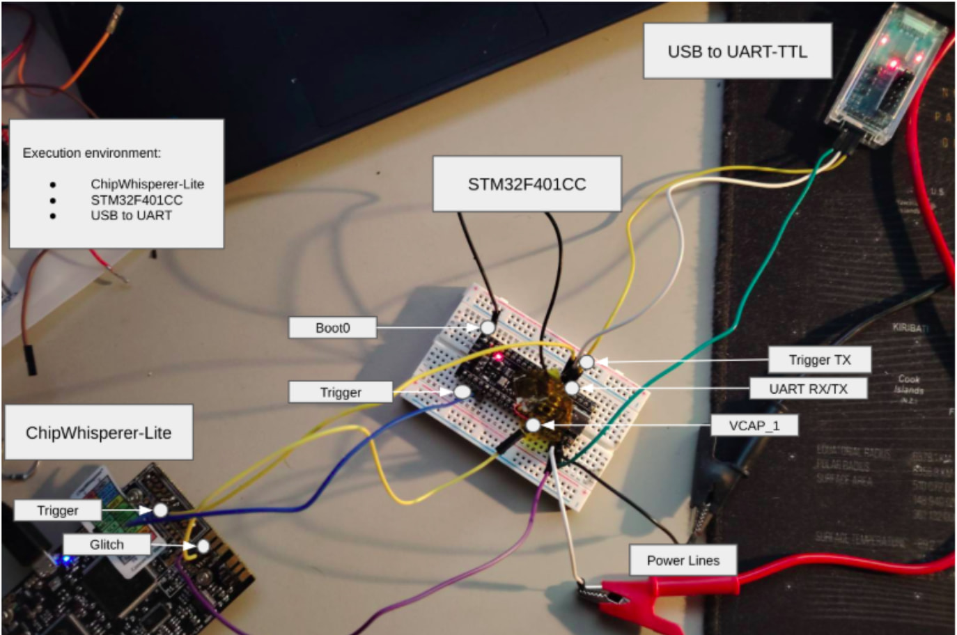
- Shaping the Glitch (TCHES: Shaping the Glitch: Optimizing Voltage Fault Injection Attacks | IACR Transactions on Cryptographic Hardware and Embedded Systems): glitching the supply at the moment the bootrom reads RDP option bytes causes the protection level to be misread. On the STM32F1, a glitch just after boot start downgrades RDP. Similar windows found on F3/F4,
- The chip.fail / Trezor Attack (STM32F2: Replicant: Reproducing a Fault Injection Attack on the Trezor One - VoidStar Security Blog): perhaps the most famous attack: glitching the Trezor One wallet’s STM32F2 approximately 170 µs into boot bypasses RDP2, exposing SRAM with wallet seeds. Famously replicated by Joe Grand for recovering significant cryptocurrency funds,
- SECGlitcher (SEC Consult, 2024: SECGlitcher (Part 1) - Reproducible Voltage Glitching on STM32 Microcontrollers - SEC Consult): built on ChipWhisperer, making voltage glitching reproducible and accessible. their conclusion: the STM32 series must be considered insecure against physical attacks when only RDP is relied upon.
- STM32L051 Flash erase suppression mechanism vulnerability (SySS, 2025: STM32L05 Voltage Glitching | SySS Tech Blog): targeting the RDP downgrade routine to suppress the flash erase while lowering protection. Risky (failed attempt erases everything), but effective,
- Glitching STM32 RDP (Anvil Secure, 2025): clean end-to-end VFI walkthrough on STM32: anvilsecure.com/blog/glitching-stm32-read-out-protection
- And many more… → fill this post with some link

(source: Glitching STM32 Read Out Protection - Anvil Secure)
In 2025, STM32-TraceRip: tracing the untraceable
At Hardwear.io USA 2025, Mark Omo and James Rowley from Marcus Engineering presented a technique called STM32-TraceRip: 100% flash recovery on the STM32G0 without any glitching, without UV light, without silicon bugs, but purely by observing the CPU state during normal execution which is smart.
First they tried recovering bytes from a CRC stored in SRAM → the Cold-Boot Stepping approach from Obermaier’s 2017 work.
The idea: if the bootloader computes a CRC over flash at startup, the intermediate CRC value sits in SRAM, which is still readable under RDP Level 1. Read it at different points in time, back-calculate the flash byte by byte.
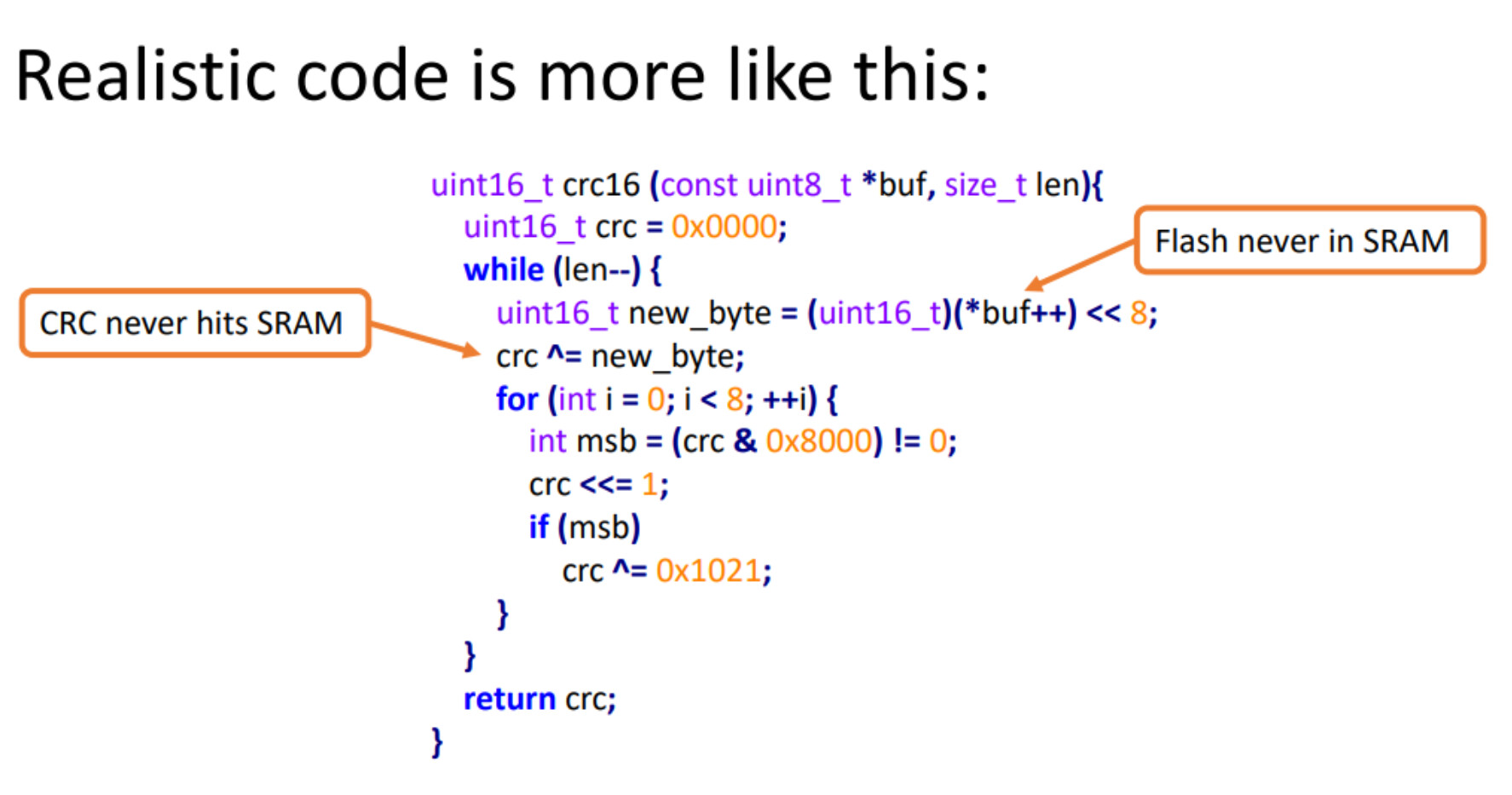
But… it didn’t work. The reason? Obermaier’s reference CRC code passed the accumulator by pointer (uint32_t * const crc), which forces the compiler to store it in SRAM. Real-world CRC implementations don’t do that → the accumulator stays in a CPU register, and flash data is fetched directly into the processor. Nothing interesting ever hits SRAM.
(source: https://hardwear.io/usa-2025/presentation/TraceRip-Hardwear.pdf)
So they redirected the attack by looking at the core behaviors instead.
The core insight
RDP Level 1 blocks debugger access to flash but still allows reading CPU core registers via the debug interface. Any bus access outside the debug block triggers a HardFault and locks flash, so no breakpoints, no single-stepping, but you can connect, cause the fault, and read the resulting CPU state.
If flash is being used, its contents are reflected in the processor state. The flash is only useful because it’s used. And if it’s used, it leaks.
So they went deeper and instead of reading SRAM, they read the CPU core registers themselves.
Probing the registers
By debuging the core, they found that the target runs a standard boot-time CRC integrity check (CRC-16/XMODEM, polynomial 0x1021) in commercial firmware.
To look for potential leaks, they used the following setup:
- Custom tooling on a Raspberry Pi Pico with modified OpenOCD firmware, and a custom DAP vendor command (
DAP_ProcessVendorCommand), - For each capture: power off target → power on in reset → configure debug block → release reset → wait precise delay → trigger bus read causing HardFault,
- Read all CPU registers (R0–R12, SP, LR, PC, xPSR…) and a small SRAM window.
- Increment delay, repeat millions of times…
The process is non-deterministic at the end, the target’s internal RC oscillator creates jitter.
But from the register data they identified:
| Register | Role |
|---|---|
| R0 | CRC accumulator (16-bit) |
| R2 | Current byte address |
| R3 | End address |
| R4 | Bits remaining to shift (0–8) |
| R5 | Polynomial (0x1021) |
| R7 | Start address |
For each CPU state snapshot produces one or more guesses of the CRC at a given address. Then:
- For each guess, compute 256 possible next-CRC values (one per possible input byte),
- Check which match guesses on adjacent bytes: creating “chains.”,
- Iteratively prune inconsistent chains forward and backward,
- Find anchor points (addresses with only one guess) and propagate certainty,
- The byte values connecting each CRC state are the flash contents.
With a 16-bit CRC, there not a lot of chance of collisio, creating ambiguous parallel chains of 20–100 bytes. These get resolved by anchors and by PC-aware refinement.
And to recover PC, they have shown that PC always reads as 0xFFFFFFFE (ARM EXC_RETURN for HardFault). But the real PC gets pushed onto the stack — in SRAM, which is readable. By grabbing the exception stack frame, they recover the actual instruction address for most frames.
Critical example: if PC points just past ldrb r1, [r2, #0x0], then R1 is the flash byte value, no CRC math needed. A single frame with a known PC can resolve an entire chain of ambiguous guesses.
Results
After collecting data across 3–5 capture runs (~2.5 days each due to the 600ms boot CRC × 50ms per capture cycle), they achieved 100% recovery of the application flash from approximately 0x08000650 to 0x0801FFFF. The first ~1000 bytes are missed due to probe startup delay, which is low-hanging fruit for improvement.
They tested on STM32F0, F1, G0, and C0 → they are all vulnerable. The RDP scheme works the same way across these families.
Key takeaways
- RDP Level 1 is not a security boundary: it’s a speed bump at best,
- RDP Level 2 can be downgraded via UV-C or voltage glitching, making Level 1 attacks applicable,
- Boot CRCs are a double-edged sword: essential for reliability, but they create a side channel. Consider using hardware CRC peripherals or running checks from RAM after decryption,
- Defense in depth: encrypt firmware at rest, use authenticated secure boot (not just CRC), implement anti-tamper, choose certified parts (SESIP/PSA Level 3+),
- For pentesters and red teamers: a Raspberry Pi Pico, some Python, and patience can now extract firmware from a wide range of deployed STM32 devices.
Lesson from TraceRip applies beyond STM32: any security model that assumes leaking processor state is safe while the processor is executing protected code is built on sand.
Resources
Slides: https://hardwear.io/usa-2025/presentation/TraceRip-Hardwear.pdf
Video: https://www.youtube.com/watch?v=eSN824_PUa0
What’s your experience attacking or defending STM32 devices? Encountered interesting protection schemes or bypasses in the wild? Drop your thoughts below!